The Next Decade
Printed and Flexible Electronics in 2010
-
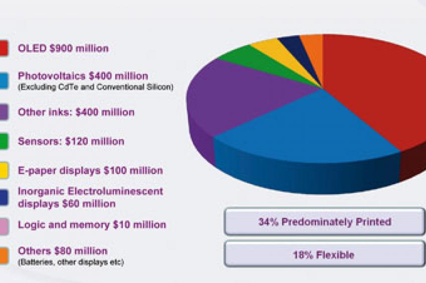 Fig. 1: The market for printed and potentially printed electronics in 2010
 -
 Fig. 2: Leading market drivers for printed electronics
 -
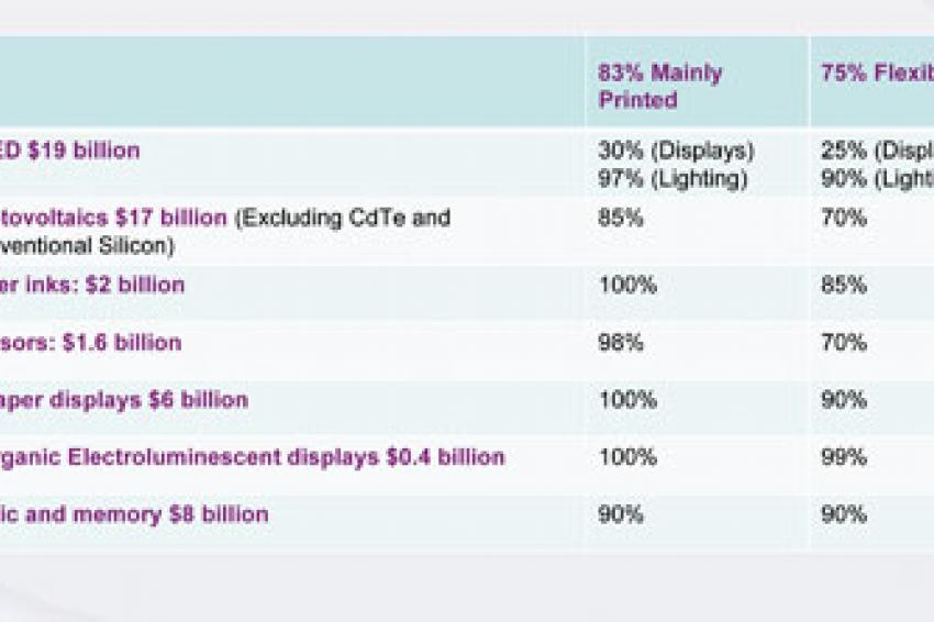 Fig. 3: The market for printed and potentially printed electronics in 2020
Exciting Developments - We have entered the second decade since the first printed electronics moved from academia to commercialization. The topic is now incredibly broad, encompassing inorganic and organic chemistries that may or may not be printed today and, judging by the many news sources now available, innovation is growing at a rapid rate. However, where are we in terms of commercialization? What is needed? Raghu Das of IDTechEx takes a look at not only the business of printed electronics, but also at exciting materials developments and opportunities.
In 2010, IDTechEx sees the size of the market as shown in table 1.
However, of the markets in 2010, less than 0.1% of the OLED market consists of flexible devices, flexible photovoltaics are 0.7% of the quoted market and only 10% of the e-paper display market is devices on flexible substrates. Flexible electronics are much more mature for the decades old AC electroluminescence (almost all is made by screen printing), and the many mature markets involving conductive ink printed for heating elements, membrane keyboards, flex connectors,etc.
2010 sees the first commercial products involving the new flexible thin film transistor chemistries - from Plastic Logic for their QUE e-reader using organic semiconductors and from Kovio that print nanosilicon onto stainless steel. This is the first commercialization of such chemistries despite over 500 organizations (academic and commercial) active in developing printed/flexible transistors. Like many other early stage technologies, both of these companies (and many others in printed electronics that have been commercially successfully so far) have moved from the left of the value chain, i.e. being involved in materials supply, to the right, selling complete products.
Chances For Consolidation
As with most other embryonic technologies, this industry is also very fragmented and there is an opportunity for consolidation. There has already been some shakeout in OLEDs over the last decade and more recently in organic semiconductors, but few are putting together complimentary technologies to build a strong value chain proposition. Companies in East Asia have been shrewd in consolidating some of the displays business, such as PVI, Sumitomo and LG.
Almost by default, developers look to replace existing electronics or devices with the new electronics that they are creating. That is proving tough given issues with yield, R&D cost that needs to be recuperated and low starting volumes. The old silicon rules such as Moore's law may not apply here - many companies today are capable of cheaply making transistor circuits with a handful of transistors - but who is exploring the useful products that can be made that incorporate a dozen transistors? High volumes can only be created with modularity and basic building blocks - but this does not necessarily mean mimicking silicon ones.
Biggest Driver is Form Factor
More so than cost or performance, IDTechEx research finds that the biggest driver of printed electronics is form factor - devices that are flexible, conformal, rollable or large area. In most of these cases, the electronics are doing something that conventional electronics cannot do or struggle to do, and therefore are usually creating new markets. Competing on cost alone is difficult - many aspects of printed/flexible electronics promise to eventually be cheaper but can often start off at a higher cost base than the incumbent technology until manufacturing volume becomes significant (fig. 1). IDTechEx3_CMI0710.emf
In 2020, IDTechEx forecast the markets to be as shown in table 2, with the value of the market that is predominately printed, or predominately flexible also indicated.
So far, role models of success are companies such as T-Ink that have used silver ink (where silver ink is in oversupply if one looks at the number of suppliers vs. demand) on 10 million McDonald's place mats, for example, or Power Paper that has created a cosmetic product using its thin flexible battery that is conformal to the body. Increasingly IDTechEx is asked by major consumer goods brands, consumer electronics and media companies for demonstrators of what the new printed/flexible electronics can do but it is surprisingly difficult to locate many. Over the next few years perhaps one indicator of success of the industry is the number of new demonstrators and products that are launched.
Materials Progress
The global recession did not slow materials development for printed electronics. In the face of the rising cost of silver, companies have developed nanosilver ink, so less silver is used, and even copper based inks, from companies such as NovaCentrix and Hitachi Chemical.
While most effort has been on organic semiconductors, display companies are now focusing on metal oxide semiconductors which have the benefit of being transparent and therefore do not block emitted light. In addition, organizations are working on nanosilicon and carbon nanotube inks as semiconductors - showing high performance.
Processing
The performance of many materials is good enough for early applications now, but there needs to be more understanding about printing these materials. If we look at conventional silicon transistors, we see that for almost 40 years the material itself used to make transistors did not change - but the drastic change in performance is attributed to higher resolution fabrication. Printing for printed electronics is still in its infancy.
Indeed, many are working now on optimizing materials for mass production rather than making gains in performance of single test devices. For example, if we look at organic photovoltaics (OPV), Konarka is now selling OPV modules made in a roll to roll process. In test conditions the cell has an efficiency of about 6% because it has a very thin active layer which is only about 100 nm thick. This prevents much of the charges that are created from the light from being recombined due to the small distance they have to travel. However, these cells are only 0.1cm2 in area - a standard size used to test the efficiency of "champion cells." In mass production, it is incredibly difficult to achieve that thickness reliably. Therefore, Konarka prints active areas which are about 200-500 nm thick. This thicker layer gives much better yield but efficiency drops to about 3% because now more charges recombine as they have to travel further to reach the electrodes.
Contact
IDTechEx Inc.
222 Third Street, Suite 222
Cambridge, MA 02142
+1 617 5777890
+1 617 5777810